Unveiling the Power 🚀️: The Crucial Role of Visualization in Understanding RISC-V Cores!
Enhancing Understanding, Debugging, and Optimization of RISC-V through Visual Insights.


Embarking on a GSoC Journey: Elevating RISC-V Cores through Visualization💡️
During the summer, I had the privilege of participating as a student in the Google Summer of Code (GSoC) program. I was fortunate to be selected by the Free and Open Source Silicon (FOSSi) organization for this exciting opportunity. I worked on the Visualization of RISC-V Cores in Makerchip Project
About GSoC
The Google Summer of Code (GSoC) is a worldwide initiative that encourages student developers to contribute to open-source software development. Managed by Google itself, the program's goal is to foster collaboration between open-source organizations and students. GSoC facilitates the application process, guides students in working on tasks, and rewards them with a generous stipend upon successful completion.
This program acts as a bridge, enabling students to join the open-source community and gain exposure to real-world software development practices. By participating, students immerse themselves in the entire development cycle, from addressing issues and fixing bugs to creating new features.
Central to open-source development is collaboration. This approach not only fuels community growth but also allows individuals to engage with experienced professionals from various sectors, be it industry or academia.
What's required to jump in? Simple: Enthusiasm and Drive.
About the Organization and My Project
My GSoC journey commenced in collaboration with The Free and Open Source Silicon Foundation (FOSSi Foundation), marking the beginning of an exciting adventure into the world of open-source silicon development.
FOSSi Foundation is a non-profit organization dedicated to promoting and advancing the use of open-source principles in the design and development of digital hardware and silicon. Founded by a group of individuals passionate about open-source hardware, FOSSi Foundation serves as a hub for collaboration, knowledge sharing, and community building within the field of open-source silicon.
My project aimed to enhance the understanding of RISC-V cores using the Makerchip platform. It emphasized the importance of visual debugging in core development, creating interactive simulations for clearer insights and more efficient issue resolution.
Understanding TL-Verilog and Makerchip: TL-Verilog, or Transaction-Level Verilog, is an emerging hardware description language (HDL) extension that aims to simplify and streamline the process of designing digital hardware.
Makerchip is a web-based integrated development environment (IDE) that focuses on the following features:
Enabling hardware and digital design engineers to create, simulate, and collaborate on complex digital systems.
Users can design hardware using hardware description languages (HDLs) such as SystemVerilog, and TL-Verilog (Transaction-Level Verilog).
Makerchip also enables features such as Interactive Debugging, Graphical Waveform Viewer, and JS-based block which is essentially integrated with Fabric.js for visualization and hierarchical diagrams.
Behind the Scenes: The GSoC Experience in Developing RISC-V Core Visualization 🌟️
Motivation
The process of comprehending, designing, and refining RISC-V cores demands a nuanced understanding of both hardware and software intricacies. Traditional methods of debugging and issue resolution often involve sifting through lines of code and cryptic registers, which can be a daunting and time-consuming task. As the complexity of RISC-V cores escalates to cater to diverse computing needs, there arises a need for innovative solutions that empower developers with tools to enhance their understanding and expedite the debugging process.
The motivation behind this project is rooted in a profound belief in the potential of the Makerchip platform to revolutionize the way we perceive and interact with RISC-V cores. By leveraging visual debugging, developers can unlock new dimensions of comprehension, bridging the gap between abstract architectural concepts and tangible insights. Visualizing the flow of data, the state of registers, and the intricate interactions within a RISC-V core can demystify complex behaviors and expedite the identification of issues.
Selection of the Core
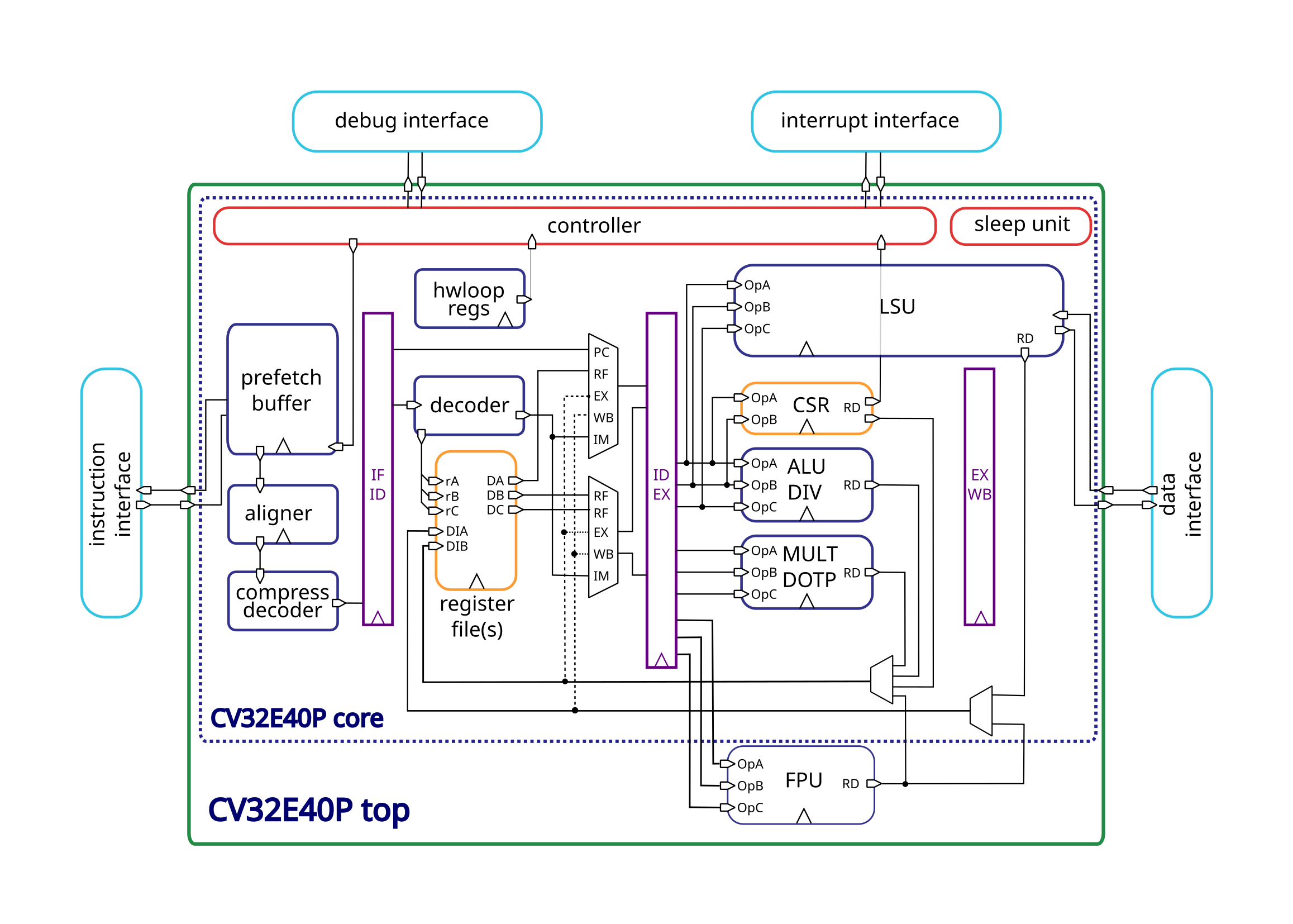
Before we began the project, we had a fundamental question: what should we show visually and how do we do it best? To figure this out, we looked at different cores used in the industry and had discussions. After brainstorming, we decided to work with the CV32E40P core, which is open-source and developed by the Open Hardware Group.
CV32E40P is a 4-stage in-order 32-bit RISC-V processor core. The ISA of CV32E40P has been extended to support multiple additional instructions including hardware loops, post-increment load and store instructions, additional ALU instructions and SIMD instructions that are not part of the standard RISC-V ISA. The figure below, shows a block diagram of the top level with the core and the FPU.
Porting the core onto Makerchip
The project's major challenge was to get the core running on Makerchip. Our primary goal was to ensure the core's functionality could run seamlessly on Makerchip, with the overarching objective of making it accessible for future endeavors and utilization.
We kicked off by bringing in the required files and fixing any errors/issues that popped up. Subsequently, we initiated the core within Makerchip's SystemVerilog section to set it in motion. For those curious, you can find a basic template of the CV32E40P core here.
The Next Steps . . .
As soon as we onboarded the core onto Makerchip, we started discussing the role of visualization and how it can impact the understanding of the core. Since I'm new to this field, the use of visual aids helped me better understand how the core functions at its most fundamental level. We initially attempted to visualize the fundamental signals to comprehend the very nature of the core.
We then shifted our focus to enhance the visualization, driving inspiration from the WARP-V core which is a versatile core and has a rich set of components for its visualization. We sought to improve our project's visual representation and to further the understanding of RISC-V cores by incorporating knowledge from the WARP-V core.
Crafting Visual Narratives: The Components of Visualisation 🧐️
After several weeks of discussion, brainstorming, and coding, we decided to depict all the pertinent architectural stages, building blocks, and interface signals in each snapshot in time. A waterfall diagram was also included to show the various steps in a particular instruction. We have also included a Disassembler in this version to assist users in decoding instructions from their binary or hexadecimal code. Here's an overview of the visualisation

Let's take a closer look at each of the components.
The Prefetch Buffer:
In general, a prefetch buffer in a processor core is a small, fast memory structure that holds instructions fetched from the main memory before they are executed by the core. This buffer allows the core to fetch and store multiple instructions ahead of the current instruction being executed.
The primary purpose of a prefetch buffer is to minimize stalls in instruction execution due to memory latency. It achieves this by fetching instructions ahead of time and storing them in the buffer so that the core has a continuous supply of instructions to execute, even if memory access times are relatively high.
For the CV32E40P core, the prefetch buffer holds in some instructions if the further stages are not ready. For this section, We included:
Number of words/instructions in the buffer: This is the count of total instructions that are currently stalled and stored in the buffer.
Current Instruction: This is a disassembled instruction that is in the buffer and is passed ahead to the IF stage when the core is ready.
Contents in FIFO: The buffer stores a FIFO type of structure to store the stalled instructions. One can check all the stalled instructions in the same order in which it is stored, this enables one to keep track of all the instructions which are waiting before entering the pipeline.
The Interfaces:
Data Interface->
The data interface of a processor core is responsible for handling data transfers between the core and the memory system. For debugging purposes, we have included:
Data Grant Signal
Data Valid Signal
Data Adress Signal
Instruction Interface->
This helps in providing the information on the instructions which are to be executed by the core. This includes:
Instruction Valid Signal
Instruction Address Signal
Instruction Decode:
This segment aids in comprehending the instruction fetched by the program counter. Each instruction is decoded using rvcodec.js, which is a RISC-V instruction set Decoder designed by UC Davis. This block provides the decoded instruction, along with its corresponding binary and hexadecimal representations, while also categorizing the instruction type based on the RISC-V instruction set architecture.
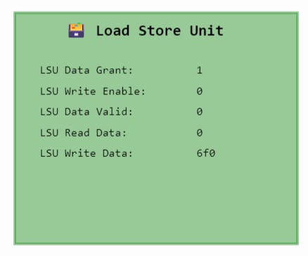
The Load Store Unit:
The Load/Store Unit is a pivotal component within the processor that handles the execution of load and store instructions in a RISC-V architecture. These instructions are responsible for transferring data between the core's registers and the main memory. The Load/Store Unit manages the intricacies of data movement, addressing, and alignment to ensure smooth and efficient memory access operations.
This block offers meaningful insights about the transfer of data through the core, These signals include:
LSU Data Grant Signal
LSU Write Enable Signal
LSU Data Valid Signal
LSU Read Data Signal
LSU Write Data Signal
The Four Stages of Pipeline:
The pipeline architecture in a processor breaks down the execution of instructions into discrete stages, allowing multiple instructions to be processed simultaneously and improving overall throughput. In this context, the pipeline is divided into four key stages:
Instruction Fetch (IF): During this stage, the processor fetches the next instruction from memory using the program counter (PC) as the memory address. The fetched instruction is then placed in an instruction register for further processing. To check the instructions in this stage, we have added a decoded instruction along with IF Valid and ID Ready Signal. This ID Ready Signal allows the processor to control the instruction flow to the next stage.
Instruction Decode (ID): In this stage, the fetched instruction is decoded to determine its type, operands, and any immediate values. The necessary control signals and resources are prepared for the subsequent execution stage. Along with the decoded instruction, ID Valid and EX Ready Signal, this stage also includes a Stall signal which controls the flow of the instruction through the pipeline.
Execution Stage (EX): The execution stage is where the actual operation of the instruction is carried out. This can involve arithmetic and logic operations, memory accesses, and branching decisions. The data values and results are processed according to the instruction type. Since ALU plays the most important role of this stage we have added the ALU Enable signal to the viz along with the LSU Enable. This block also includes EX Valid Signal.
Write-Back (WB): In the final stage, the results of the execution are written back to the appropriate registers. This includes updating destination registers with computation results or loading data from memory into registers in the case of load instructions. For this last stage, we have incorporated, WB Ready, WB Contention and a Register File Write Enable Signal.
The Register View 📑️:
Registers in RISC-V architecture are crucial components used for storing data, addresses, and intermediate results during program execution. The 3 major components included in the visualization are:
Register File: CV32E40P has 31 32-bit wide registers which form registers
x1tox31. Registerx0is statically bound to 0 and can only be read, it does not contain any sequential logic. The register file has three read ports and two write ports. Register file reads are performed in the ID stage. Register file writes are performed in the WB stage.Control and Status Registers: These registers are crucial for controlling various aspects of the processor's behavior, privilege levels, and exception handling. They also provide status information about the core's operation. CSRs are used for tasks like enabling/disabling interrupts, accessing performance counters, and managing virtual memory settings.

The Memory View 💠️:
The Data Path RAM (DP RAM) in the context of the CV32E40P core refers to a dedicated memory component within the core that is used to store data during the execution of instructions. This type of RAM is closely associated with the core's data path, which is responsible for performing arithmetic, logic, and data movement operations. The long memory view is divided into 8 columns to enhance visibility.
The Instruction Memory 📝️:
This perspective compiles a comprehensive list of instructions slated for execution throughout the program's lifecycle. This compilation offers an overarching understanding of the program's anticipated operations. To facilitate debugging and scrutinize the program's flow, the instruction currently residing in the program counter is accentuated.

The Waterfall Diagram 🌊️:
The Waterfall Diagram illustrates a sequential and hierarchical representation of the signal propagation and data flow within a digital system. It is a visual tool that aids in understanding the progression of signals through various logic stages, providing insights into the timing, dependencies, and interactions between different components.
This diagram showcases how input signals evolve as they traverse through different levels of logic gates, flip-flops, and other digital components. The name "Waterfall" is derived from the descending nature of signal propagation, resembling the cascading flow of water.
Here's a Link to my Makerchip Sandbox: CV32E40P Viz
Future Prospects: Paving the Way for Ongoing RISC-V Core Visualization Advancements ✨️
As the realm of RISC-V core visualization continues to evolve, exciting prospects and opportunities emerge, promising to enhance the understanding, development, and optimization of RISC-V cores.
Visualization serves as both a simplification aid for comprehending core functionality and a valuable asset during core debugging. I consider visualization a true blessing, as it significantly enhanced my grasp of signals and architecture efficiency, despite my limited knowledge of Hardware design. Visual representations not only simplify intricate core operations but also facilitate smoother debugging processes, making it an indispensable tool in my experience.
I'd like to express my gratitude to my mentors, Steve Hoover and Bala Dhinesh, for their unwavering guidance and support throughout this journey. A heartfelt thank you goes out to FOSSi for providing me with this incredible opportunity. Additionally, I want to extend my appreciation to Shrihari for his assistance in both the core setup and enhancing my comprehension of its intricacies.